.
.
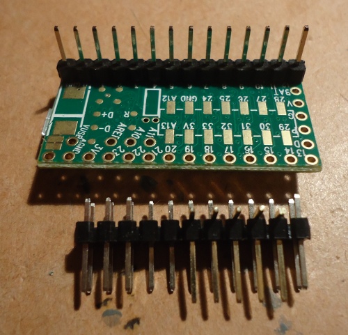
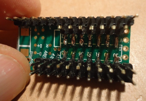
A much better idea to use a double header with straight pins replaced by right angle pins.
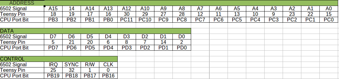
The Teensy has 34 digital I/O pins that are connect across the ARM processor GPIO pins/ports. I wanted to keep the 6502 signals connect in sequence on the ARM ports so that direct port reads would give the full address and data bits. The plan is to read the address/data/control signals are read on the second half of the 6502 clock cycle (phase 2 clock high). With the 6502s 1Mhz clock there is 0.5 microsec (500nsec) available to read and store the data. It is important to keep the time required to read the 6502 signals to a minimum and having the 6502 signals sequentially connected to the ARM ports would help this.
However the Teensy GPIO pins are distributed across Port A thru E. I decided to use most of Port C for the address, Port D for the data, and Port B for control and the rest of the address bits.
.
.
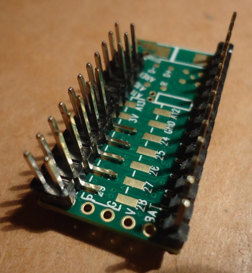
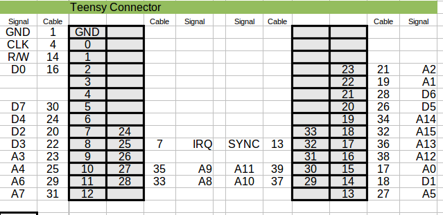
Pin out for the front side wiring:
.
.
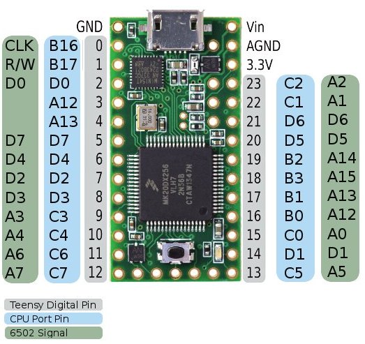
Pin out for the back side wiring:
This layout allows three direct port reads to get the 6502 signals. We need to bit shift a few things to have the bits in the right places.
// read Ports C, B, and D
addr =  GPIOC_PDIR & 0x0FFF;
addr_ctrl =  GPIOB_PDIR ;
data =  GPIOD_PDIR & 0x00FF;

// shuffle bits around to get seperate address and control signals
address = addr | ((addr_ctrl & 0x000F) << 12) ;
rw   = (addr_ctrl & 0x00020000) >> 17;
sync = (addr_ctrl & 0x00040000) >> 18;
irq  = (addr_ctrl & 0x00080000) >> 19;
With just three reads, some bit rearrangements, and storing the results the Teensy is able to complete each capture cycle in approximately 0.5 micro sec (500nsec). The 6502 clock is just starting into the next cycle (phase 2 low) and the Teensy is ready for the next record. This would not work with a 2MHz or 4MHz 6502 (or any of the fancy new 14MHz ones).
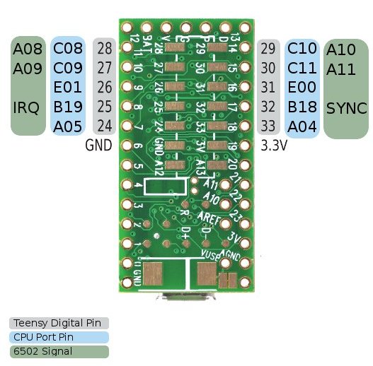
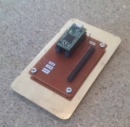
The 28 I/O pins are wired to a 40 pin ribbon cable connector. I also wired out a few test points from the Teensys pins 3 and 4. The software toggles pin 4 high when it finds the trigger address and starts recording data. Pin 3 toggles on during each capture cycle. These pins can be connected to a Saleae logic analyser and view timing of the record cycle.
The most difficult part of wiring this was to get the pins of the backside of the Teensy wired. I started to wire the Teensy pins with individual headers then I found the discussion on the Teensy forum on how to use double row headers and replace some of the straight pins with right angles ones. This provide a much stronger approach so you are not pulling the connectors off the board as it is removed from a socket.
From the PJRC Teensy Forum
After breaking off one 2x14 section of the dual header, I carefully removed
seven of the straight pins from the inner section, and replaced them with 7
right-angle pins that I carefully removed from the right angle header. I also
removed the two pins that are next to VIN and 3.3V on the inside. I trimmed the
right angle pins to cover just the pads on the underside of the Teensy3.x.

And solder everything with a fine-tipped soldering iron. The dual headers
add some mechanical rigidity, and allows the Teensy3.x to be used with a
socket..
.
The initial start at wiring one side with individual headers
.
.
A much better idea to use a double header with straight pins replaced by right angle pins.
.
.
All pins ready to go ... and yeah I know the soldering is a bit sloppy
.
.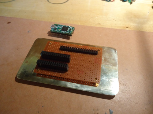
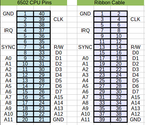
The Teensy socket is wired to the ribbon connector on the back of the perf board using point-to-point wiring.
.
.
The Teensy socket layout:
.
.
The Ribbon Connector layout mirrors the 6502 pin layout:
There are three programs for this system; "la65" is the logical analyser code that runs on the Teensy, "cli65" is the command line used to control the Teensy, and "t65" is for trace/disassemble of captured data.
You can find the code on github
Most of the code in this program is associated with receiving commands from the linux host. The core of the logic Analyser is in the "xrun" function. The first section of this program is a while loop that waits for the trigger address: while + wait for phase 2 clock to go low -this is the start of CPU read/write cycle +wait for phase 2 clock to go hi - now we read the 6502 signals + if the address equals the trigger record data as first sample + else loop
The second while loop is essentially the same thing except in this loop we read the data lines twice to ensure the data is valid. The 6502 actually reads the data on the falling edge of the phase 2 clock and expects the external device (RAM) to hold the data valid for 50nsec. Since we are doing this in software 50nsec if too short to detect the falling edge of the clock and then read the data. Instead I have inserted a few NOPs to delay the data read the data during the later half of the clock cycle. Not a perfect solution but it is working.
Here is the whole read and record process that runs as soon as the 6502 clock goes high.
digitalWriteFast(TESTPIN1, HIGH);
// read address and control line bits
addr =  GPIOC_PDIR & 0x0FFF;
addr_ctrl =  GPIOB_PDIR ;
address = addr | ((addr_ctrl & 0x000F) << 12) ;

rw   = (addr_ctrl & 0x00020000) >> 17;
sync = (addr_ctrl & 0x00040000) >> 18;
irq  = (addr_ctrl & 0x00080000) >> 19;


// read data last as it takes memory a while to present it
__asm__ __volatile("NOP");
__asm__ __volatile("NOP");
__asm__ __volatile("NOP");
__asm__ __volatile("NOP");
__asm__ __volatile("NOP");
data0 =  GPIOD_PDIR & 0x00FF;
__asm__ __volatile("NOP");
data =  GPIOD_PDIR & 0x00FF;
if (data != data0) {
    fail = TRUE;
    done = TRUE;
}

// address, data and control bits saved into one 32 bit arrary
bits[head++]=address | (data << 16) | (rw<<24) | (sync<<25) | (irq<<26);
if(head >=BUFFERSIZE)  done=TRUE;

// turn off test pin to show we are done reading data
digitalWriteFast(TESTPIN1, LOW);
In this image shows the system at the start of the trigger.
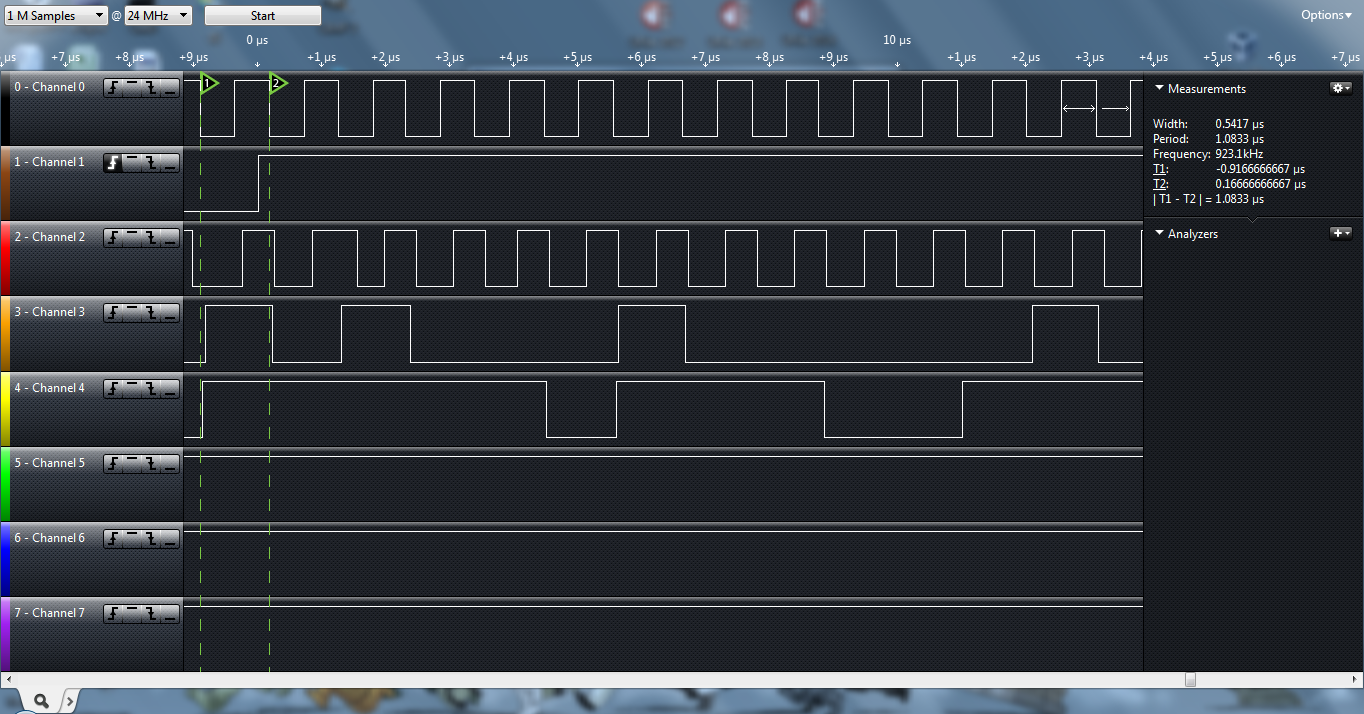
The read/record test pin goes high just after the CPU clock. It is high for approximately 500nsec while the Teensy reads and stores the address, data, and control signals.
This program is a small command line interperter that send commands to the Teensy via the serial port (it is really over USB but this code do not know that).
There are a few quirks with this program. If you put the Teensy into a run and record cycle there is not way to break out of it other than reset the Teensy. Since interrupts are shutoff on the Teensy during the record function the only exit is a hard reset. If the trigger address does not arrive the Teensy will spin forever.
If this program is running when the the Teensy is reset the normal serial port (/dev/ttyACM0) will be busy. The Teensy will be slotted into /dev/ttyACM1. This causes no end of confusion.
Just what the world need is another 6502 disassembler. But it was a long cold snowy winter in New Brunswick last year and that resulted in yet another disassembler. I modified it a bit to show memory reads and writes in addtion to the instructions & opcodes.
2015/11/25